
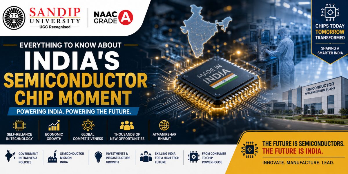
Unlocking your phone, tapping on the UPI link on your phone’s screen or hailing an electric scooter to get to work is how most of us tech-savvy Indians start our day. And powering all of these is something you can’t see in semiconductor chips, made of pure silicon, that form the core of every modern product. And now, in 2026, it’s ‘Chip Moment’ for India as it bets big on a semiconductor ecosystem that’s going to be made in India.
Let us discuss semiconductor chips and how India is building a semiconductor ecosystem in 2026 and how Indian students from some of the best engineering colleges in Nashik can make a career in this field.
What is an integrated circuit?
A semiconductor chip comprises a small piece of silicon. It controls and processes the electric signals. Think of it as the “brain” of the “nerves” in electronics. Potato chips are inside. Mobile phones, computers. Television, internet routers and home appliances. Vehicles, healthcare machinery, and factory equipment. First, they are designed by chip design engineers using special software. Then, they are produced in highly advanced factories which are more commonly known as fab which is short for fabrication units. Finally, they are packaged and tested before you find them in the products you use.
What makes 2026 a “chip moment” for India?
A highly determined national approach with assured finance: The India Semiconductor Mission is a government initiative to develop a semiconductor ecosystem in India comparable to international levels. The revised semiconductor and display manufacturing scheme under Union Budget 2026-27 plans to commit a fund of around INR 8,000 crore towards this and a fund of INR 1,000 crore will be allocated towards ISM 2.0 to encourage research, training and skilling. ISM would support the complete value chain: Semiconductor fabrication (foundry) plants; Assembly, Testing, Marking & Packaging (ATMP) units; Designing chip products; Making complex semiconductors, sensors and advanced packaging; Developing chips and creating an enduring high-quality engineering job environment.
New fabs and facilities on the ground
The article talks about the Semiconductor chips and how India is planning a ‘Semiconductor Ecosystem’ in the Year 2026. Also, it elaborates on how Indian students can make a career in the same. It packages and tests advanced DRAM and NAND memory chips. It is anticipated to generate over 20,000 jobs direct and indirect. Semiconductor fab at Dholera, Gujarat, with Taiwan’s PSMC. by roughly INR 91,000 crore of investment. AI-capable plant for 300mm wafers. The high-volume trial runs and process validation will begin in early 2026 with the first silicon expected by late 2026. It will employ about 21000 people. Tata has a plant for assembly and testing in Jag Road, Assam. Already in operation, focusing on semiconductor assembly and testing. Not promises for the future; these are facilities that are starting production and hiring now.
Hiring surge across the chip stack
Companies are actively recruiting for Design and verification of chip Process/fab engineering ATMP/OSAT operations. Similarly, combined ATMP and OSAT work resulted in even more excessive grid usage. This high utilisation was mainly due to the fact that the 5, the 3, and the 2 processes had too much work to be processed at each stage of the facilities. Embedded systems and firmware. He shall master the equipment, the yield, the quality and the reliability engineering. Notable is the influx of fresher recruits from engineering colleges in India especially in design, verification and ATMP roles. India is aiming at hundreds of thousands perhaps in the range of one million semiconductor associated jobs by the end of this decade as the ecosystem expands. For students this means: the chip industry is no longer an unachievable dream. It is a reality, and one that is now beginning to reach campuses across India.
Top semiconductor career paths
You need not be from the same branch. ECE, EEE, EIE, CSE are also having this opportunity.
-
Chip design / VLSI design
Create digital and analogue circuits for integration onto a chip. Use hardware description languages (Verilog, VHDL, etc.) and design tools supplied by Cadence, Synopsys and other support companies. Common job: Digital design engineer, analog design engineer, physical design engineer.
Background: Good fundamentals in digital electronics, signals and computer architecture.
-
Verification and validation
Your tasks: Debugging chip designs, and looking for problems with the design before it is manufactured. Writing testbenches, and testing the design using a simulator. Common positions: Design validation engineer, verification engineer.
Background: Good logic, scripting (Python/Perl/Tcl) skills, knowledge in digital systems.
3.Fabrication/process engineering
Inside fabs, on the actual manufacturing process. Cleanroom handling, process monitoring, yield improvements. Typical roles responsible in any product or process support area: process engineer, equipment engineer, yield engineer.
Background: love of physics, materials, lab work. Often best for ECE/EEE/EIE but want manufacturing.
-
ATMP (Assembly, Testing, Marking, Packaging)
Bring the final step in chip manufacture to completion the packaging of the silicon die, testing, marking, and quality control. Common job titles: ATMP engineer, test engineer, packaging engineer.
Background: Understanding of electronics, enthusiasm for production and quality processes.
-
Embedded systems and firmware:
Develop embedded code that executes on chips and microcontrollers. Develop for IoT equipment, vehicles, consumer devices and industrial systems. Common functions: Embedded software engineer, firmware engineer, IoT engineer.
Background: Good in C/C++, have some understanding of microcontrollers, basic electronics. Very suitable for CSE/ECE/EEE students.
Challenges in India’s semiconductor push
India’s semiconductor mission is perhaps one of the most ambitious for the country so far in terms of technology. Nevertheless, despite the grand vision, there are several risks that are involved in the mission.
-
Huge capital and long gestation periods
Establishing a fab for semiconductors is highly costly. An integrated, state-of-the-art one typically costs between USD15–20 billion and requires 4–5 years to scale to full production. This causes a lot of apprehension among investors even with government backing.
-
Infrastructure requirements
power, water, cleanrooms Semiconductor fabs need: Power that is unfailingly, ultra stably reliable (approximately 99.9999% uptime) Hundreds of thousands of litres of ultrapure water per day Class1 cleanrooms sand dedicated wastes treatment systems Indeed, a lot of those Indian industrial zones are still at the “fab grade” stage at the moment. A few areas are still affected by some water stress and electric power shortages.
-
Dependence on imported materials and equipment
India currently imports most of the critical inputs for chip manufacturing: Speciality chemicals and gases since a telephone call. Silicon wafers, photoresists, and etchants, etc. More advanced lithography and process equipment Over 90% of them are imported from outside India, thus leading to increased costs and supply chain risks.
-
Global competition and technology restrictions
Group of players such as Taiwan, South Korea and the US have already established dominance over sufficiently advanced chip manufacturing/processing. Furthermore. export controls have limited access to the most advanced node of process (ex sub7 nm), thus also slowing down India’s transition into the cutting-edge node of processing.
Conclusion
India’s semiconductor story of 2026 is no more a document of policy or a headline of the news. With live fans, new ATMP plants and a defined national mission underway, it is building the long-term chip ecosystem. The issues of enormous capital and infrastructure requirements, reliance on imports, skill and talent gaps are sizable. But they are also where the largest opportunities are for engineers, researchers and startups like.
For students, it is arguably the most exciting field of engineering in this decade from design, fabrication, testing, embedded systems, to many other capabilities. You don’t need to become an expert today. Pick just one relevant course, one project or one internship in VLSI, embedded systems or hardware. Talk to professors, track industry trends. Constantly enhance your expertise around this ecosystem. India is creating its chip future. It is not whether this field will grow for the next generation of engineers from some of the best engineering colleges in Maharashtra, it’s whether they will be a part of that growth.